Introduction to TEM Grids
Transmission Electron Microscopy (TEM) grids are the backbone of nanoscale research, enabling scientists and engineers to push the boundaries of nanotechnology. By serving as stable supports for specimens, TEM grids enable visualization of atomic and molecular structures with extraordinary clarity. This precise imaging is fundamental to advancing our understanding of how materials behave, interact, and transform at the most minor scales.
From analyzing semiconductor components to characterizing biological specimens, TEM grids provide unprecedented detail. The nanotechnology revolution owes much of its progress to the consistency and adaptability provided by these tiny, yet critical, platforms. High-performance TEM grids facilitate accurate sample positioning—ensuring even the most delicate nanostructures remain intact during examination while minimizing contamination and artifacts commonly found in other mounting approaches.
One of the most significant advantages of TEM grids is their versatility. Available in a variety of mesh sizes, hole patterns, and materials, these grids can be tailored to suit the unique requirements of particular samples and imaging techniques. This adaptability helps drive research in materials science, chemistry, and the life sciences, accelerating breakthroughs across industries.
In addition, advances in grid design continue to eliminate barriers in nanoscale research. For example, modern grids can withstand increasingly high voltages and beam intensities, resulting in sharper imaging of even the smallest particles. Such improvements are instrumental for cutting-edge applications, including drug delivery systems and innovative electronics, where a deep understanding of nanoscale features is vital.
Advancements in TEM Grid Technology
Recent years have seen a rapid evolution in the design and fabrication of TEM grids. State-of-the-art grids now use advanced materials like graphene and silicon nitride, enhancing both stability and conductivity for transmission electron microscopy. These materials boost not only the durability of the grids but also their imaging performance, paving the way for clearer, high-contrast images of nanoparticles and biomolecules.
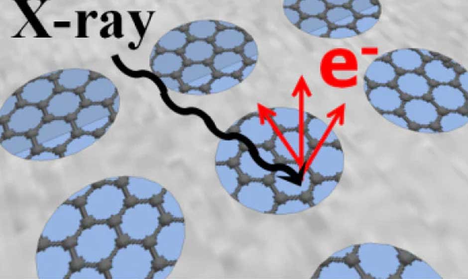
One remarkable breakthrough in TEM grid technology is the development of self-assembling coatings formed from two-dimensional nanosheets. These innovative coatings offer a substantial increase in shelf life and chemical resistance, making them particularly valuable for long-term studies and repeated experiments.
In practice, newer TEM grids yield lower background noise and better sample visibility. This is especially important when only trace molecules or delicate biological assemblies are being studied. As a result, scientists can now push the limits of what is observable, revealing critical insights previously obscured or unattainable.
Role of TEM Grids in Nanoparticle Research
TEM grids sit at the heart of nanoparticle research. By enabling real-time imaging of nanostructures, they allow researchers to witness the self-assembly and growth of nanoparticles as they happen. This live monitoring is crucial for fields such as catalysis, energy storage, and nanomedicine, where the function and efficiency of materials depend upon their precise morphology and arrangement.
Recent studies have used liquid-phase TEM to capture nanoparticles as they spontaneously organize into crystalline arrays, providing a newfound understanding of particle interactions and energy-minimization strategies. Such insights are key in designing next-generation materials with tailored mechanical, optical, or electronic properties. By mastering these processes, researchers can develop custom nanostructures for targeted applications, including more efficient catalysts, responsive nanodevices, and scalable electronic components.
Impact on Sustainable Manufacturing
Enhanced TEM grid technology is critical in the journey towards sustainable manufacturing. Through detailed imaging and precise analysis of nanoscale building blocks, researchers can design and develop materials that switch their properties in response to environmental inputs. This adaptability is driving the rise of innovative coatings and eco-friendly manufacturing processes that enable materials to transition seamlessly between different functional states, reducing resource waste while maximizing performance.
Innovative adaptive materials—such as shape-shifting nanoparticles for programmable surfaces and responsive packaging—are enabled by real-time structural insights from advanced TEM grid analysis. These capabilities facilitate the engineering of lighter, stronger, and more energy-efficient products, supporting the global push toward greener, more sustainable technologies.
Contribution to Smart Adaptive Materials
TEM grids have become central to the exploration and creation of innovative adaptive materials. By allowing scientists to probe structural dynamics and monitor the real-time response of materials under various stimuli, they enable the design of systems that behave predictably in changing environments. Applications for these materials range from flexible electronics and medical implants to next-generation sensors and actuators.
For instance, research into responsive polymer nanocomposites—materials that alter their shape, color, or conductivity when subjected to heat, light, or electric fields—would not be possible without the atomic-resolution imaging capabilities offered by state-of-the-art TEM grids. As material complexity increases, the ability to characterize nanoscale interfaces and monitor transitions continuously will remain invaluable.
Future Prospects
The rapid progression of TEM grid technology points to an exciting future in nanotechnology. Continued improvements in grid composition, strength, and imaging clarity will allow researchers to unlock new applications that remain out of reach today. The ongoing integration of machine learning and AI for automated image analysis will further accelerate discoveries, enabling the rapid screening of thousands of nanostructures for ideal properties.
Further down the road, breakthroughs in adaptive and customizable grids could facilitate the study of increasingly complex systems—think living cells, quantum materials, and even artificial intelligence-enabled nanoscale machines. By combining high-resolution imaging with vast analytical power, the next generation of TEM grids will be key to unlocking the full potential of nanotechnology across all sectors.
Conclusion
TEM grids are the silent enablers of the most groundbreaking discoveries in nanotechnology. Their evolution—from simple support films to sophisticated, engineered platforms—has been instrumental in advancing imaging, material design, and sustainability. As the field evolves and new challenges emerge, TEM grids will remain core to both understanding and harnessing the capabilities of the nanoscale world, shaping innovations that redefine industries for decades to come.